Global Wafer Level Packaging Market Size to worth USD 37.85 Billion by 2033
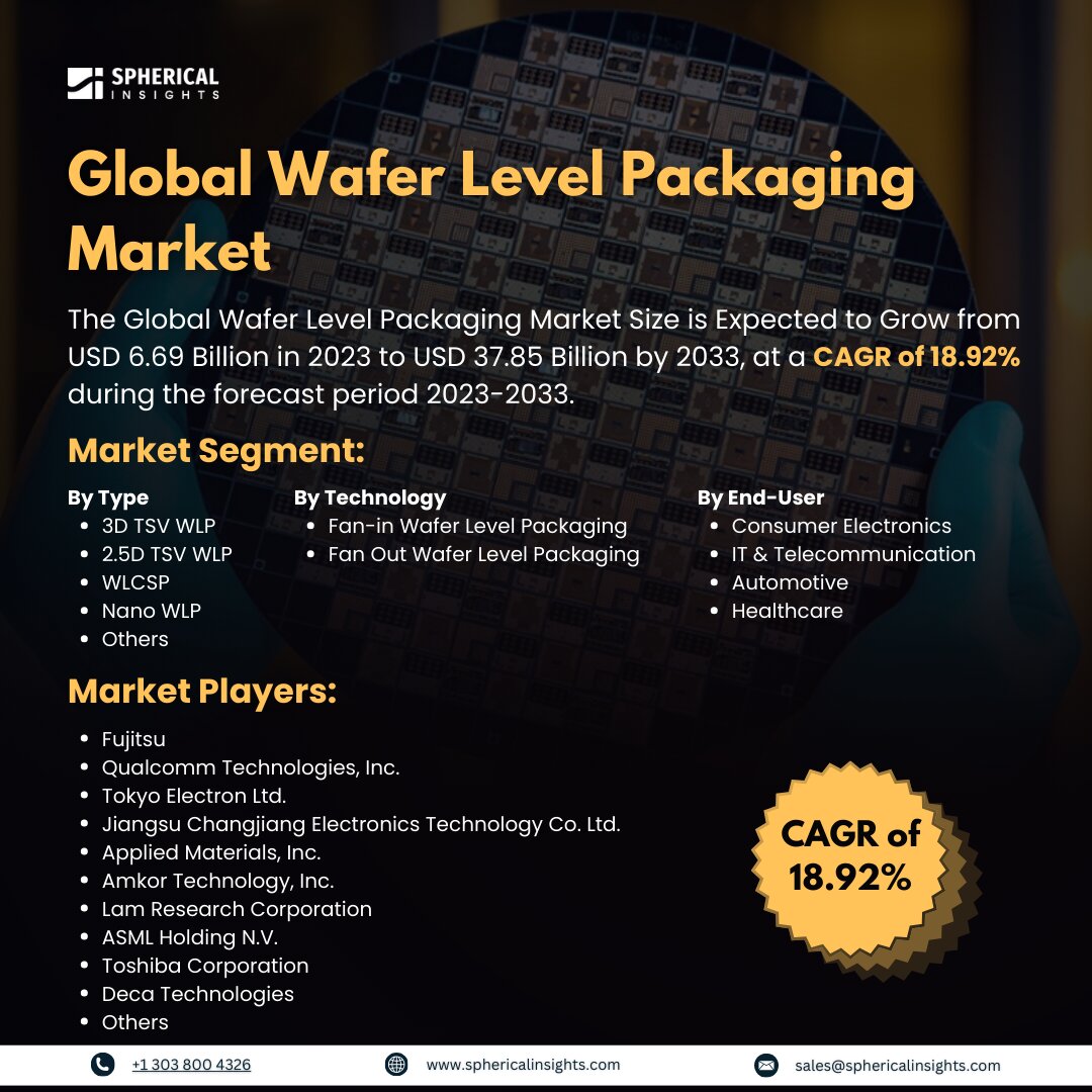
According to a research report published by Spherical Insights & Consulting, the Global Wafer Level Packaging Market Size is Expected to Grow from USD 6.69 Billion in 2023 to USD 37.85 Billion by 2033, at a CAGR of 18.92% during the forecast period 2023-2033.
Browse key industry insights spread across 210 pages with 110 Market data tables and figures & charts from the report on the Global Wafer Level Packaging Market Size, Share, and COVID-19 Impact Analysis, By Type (3D TSV WLP, 2.5D TSV WLP, WLCSP, Nano WLP, and Others), By Technology (Fan in Wafer Level Packaging and Fan Out Wafer Level Packaging), By End-User (Consumer Electronics, IT & Telecommunication, Automotive, and Healthcare), and By Region (North America, Europe, Asia-Pacific, Latin America, Middle East, and Africa), Analysis and Forecast 2023 – 2033.
Wafer level packaging market involves the connection of components to an integrated circuit (IC) before is diced. The packaging provides a compact high-performance solution for semiconductor packaging, revolutionizing the way electronic devices are designed and manufactured. The increasing usage of semiconductor ICs in the Internet of Things (IoT) along with the adoption of 3G/4G/5G telecommunication standards, government incentives to use energy-efficient systems & solutions, and advancement in wired & wireless communication technologies are the factors driving the market growth. Further, the rising panel-level packaging is propelling the market expansion. On the contrary, the complexities associated with the manufacturing processes are responsible for restraining the market.
The 2.5D TSV WLP segment dominated the market with the largest share of the wafer level packaging market in 2023.
Based on the type, the global wafer level packaging market is divided into 3D TSV WLP, 2.5D TSV WLP, WLCSP, Nano WLP, and others. Among these, the 2.5D TSV WLP segment dominated the market with the largest share of the wafer level packaging market in 2023. Due to its increased capacity, reduced system space requirements, greater performance, and low power consumption, the 2.5D TSV WLP is extensively used.
The fan in the wafer level packaging segment dominates the global wafer level packaging market during the forecast period.
Based on the technology, the global wafer level packaging market is divided into fan-in-wafer level packaging and fan-out-wafer level packaging. Among these, the fan in wafer level packaging segment dominates the global wafer level packaging market during the forecast period. Fan-in wafer level packaging technology is known for its compact size and cost-effectiveness which is an ideal choice for small devices.
The consumer electronics segment is dominating the global wafer level packaging market during the forecast period.
Based on the end-user, the global wafer level packaging market is divided into consumer electronics, IT & telecommunication, automotive, and healthcare. Among these, the consumer electronics segment is dominating the global wafer level packaging market during the forecast period. The widespread usage of WLP in consumer electronics including smartphones, tablets, and smartwatches is driving the market expansion.
North America is projected to hold the largest share of the global wafer level packaging market over the forecast period.
North America is projected to hold the largest share of the global wafer level packaging market over the forecast period. The surging need for energy-efficient, increased-performing, and small-form-factor packages where WLP is increasingly used in devices like smartphones is driving the market. Further, the presence of leading semiconductor companies and technological advancements are contributing to promoting the market.
Asia Pacific is predicted to grow at the fastest CAGR in the wafer level packaging market over the forecast period. India’s expanding smartphone adoption is significantly driving the regional market growth. Further, the continuous advancements in packaging technologies including 3D wafer level packaging are propelling the market growth in the region.
Competitive Analysis
Major key players in the wafer-level packaging market include Fujitsu, Qualcomm Technologies, Inc., Tokyo Electron Ltd., Jiangsu Changjiang Electronics Technology Co. Ltd., Applied Materials, Inc., Amkor Technology, Inc., Lam Research Corporation, ASML Holding N.V., Toshiba Corporation, Deca Technologies, and Others.
Key Target Audience
- Market Players
- Investors
- End-users
- Government Authorities
- Consulting And Research Firm
- Venture capitalists
- Value-Added Resellers (VARs)
Recent Developments
- In March 2023, Advanced Semiconductor Engineering, Inc. (ASE), a member of ASE Technology Holding Co., Ltd., announced its most advanced Fan-Out-Package-on-Package (FOPoP) solution, developed to lower latency and deliver exceptional bandwidth advantages for the dynamic mobile and networking markets.
Market Segment
This study forecasts revenue at global, regional, and country levels from 2023 to 2033. Spherical Insights has segmented the global wafer level packaging market based on the below-mentioned segments:
Global Wafer Level Packaging Market, By Type
- 3D TSV WLP
- 2.5D TSV WLP
- WLCSP
- Nano WLP
- Others
Global Wafer Level Packaging Market, By Technology
- Fan-in Wafer Level Packaging
- Fan Out Wafer Level Packaging
Global Wafer Level Packaging Market, By End-User
- Consumer Electronics
- IT & Telecommunication
- Automotive
- Healthcare
Global Wafer Level Packaging Market, Regional Analysis
- North America
- Europe
- Germany
- Uk
- France
- Italy
- Spain
- Russia
- Rest of Europe
- Asia Pacific
- China
- Japan
- India
- South Korea
- Australia
- Rest of Asia Pacific
- South America
- Brazil
- Argentina
- Rest of South America
- Middle East & Africa
- UAE
- Saudi Arabia
- Qatar
- South Africa
- Rest of the Middle East & Africa