Global Indium Phosphide Wafer Market Size To Worth USD 565 Million By 2033 | CAGR Of 13.46%
Category: Chemicals & MaterialsGlobal Indium Phosphide Wafer Market Size To Worth USD 565 Million By 2033
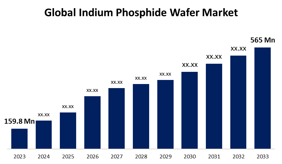
According to a research report published by Spherical Insights & Consulting, the Global Indium Phosphide Wafer Market Size is to Grow from USD 159.8 Million in 2023 to USD 565 Million by 2033, at a Compound Annual Growth Rate (CAGR) of 13.46% during the projected period.

Get more details on this report -
Browse key industry insights spread across 231 pages with 110 Market data tables and figures & charts from the report on the " Global Indium Phosphide Wafer Market Size, Share, and COVID-19 Impact Analysis, By Diameter (2 Inches, 3 Inches, and 4 Inches and above), By Type (P-Type and N-Type), By Application (Consumer Electronics, Telecommunication, Healthcare), and By Region (North America, Europe, Asia-Pacific, Latin America, Middle East, and Africa), Analysis and Forecast 2023 – 2033." Get Detailed Report Description Here: https://www.sphericalinsights.com/reports/indium-phosphide-wafer-market
An indium phosphide (InP) wafer, made from indium and phosphorus, is a III-V semiconductor used in high-power and high-frequency electronics and photonics. It has superior electron velocity compared to silicon and gallium arsenide. InP wafers are produced via methods like MOCVD or MBE and are used in high-electron-mobility transistors, laser diodes, photodetectors, and integrated circuits. Its high electron mobility ensures faster operation, while its direct bandgap aids efficient photon emission and absorption, making it ideal for optoelectronic applications like photonic integrated circuits, lasers, and high-efficiency solar cells. InP's thermal stability enhances reliability. The market growth for indium phosphide (InP) wafers is driven by their superior electronic and photonic properties, essential for high-speed and high-frequency devices, and the rising demand for advanced communication systems like 5G and photonic integrated circuits. Expanding applications in optoelectronics, such as high-efficiency solar cells and laser technologies, along with advancements in semiconductor technology and R&D in consumer electronics, further propel the market. However, the global indium phosphide (InP) wafers market faces challenges like complex manufacturing processes and scarce raw materials, competition from alternative semiconductors like silicon, GaAs, and GaN, and limited advanced fabrication facilities.
The 4-inch and above segment is anticipated to hold the greatest share of the global indium phosphide wafer market during the projected timeframe.
Based on the diameter, the global indium phosphide wafer market is divided into 2 inches, 3 inches, and 4 inches and above. Among these, the 4-inch and above segment is anticipated to hold the greatest share of the global indium phosphide wafer market during the projected timeframe. Larger diameter wafers enhance production efficiency by allowing more chips per wafer and lowering unit costs, with advancements in manufacturing equipment making them more feasible and cost-effective. The adoption of 4-inch and larger wafers in high-frequency and high-power applications, like telecommunications and photonic integrated circuits, boosts this segment's growth.
The n-type segment is anticipated to hold the greatest share of the global indium phosphide wafer market during the projected timeframe.
Based on the type, the global indium phosphide wafer market is divided into p-type and n-type. Among these, the n-type segment is anticipated to hold the greatest share of the global indium phosphide wafer market during the projected timeframe. N-type indium phosphide wafers, known for high electron mobility and saturation velocity, are ideal for high-speed and high-frequency applications, used in transistors, lasers, and photodetectors. Their high thermal stability and performance in diverse conditions make them attractive for industrial and commercial uses, especially in telecommunications and defense.
The consumer electronics segment is anticipated to grow at the fastest pace in the global indium phosphide wafer market during the projected timeframe.
Based on application, the global indium phosphide wafer market is divided into consumer electronics, telecommunication, and healthcare. Among these, the consumer electronics segment is anticipated to grow at the fastest pace in the global indium phosphide wafer market during the projected timeframe. The rapid growth is driven by the demand for high-performance, energy-efficient devices, with indium phosphide wafers crucial for high-speed transistors, lasers, and photodetectors in smartphones and wireless communication. Advances in technology, consumer preferences for enhanced connectivity, and the expanding market for wearables and IoT boost their adoption.
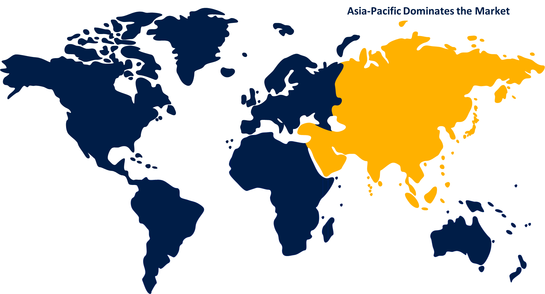
Asia Pacific is anticipated to hold the largest share of the global indium phosphide wafer market over the forecast period.

Get more details on this report -
Asia Pacific is anticipated to hold the largest share of the global indium phosphide wafer market over the forecast period. This region is a global semiconductor manufacturing hub, home to leading electronics companies. Also, there have been significant investments in technology and infrastructure across China, Japan, South Korea, Taiwan, and India. The tech-savvy population drives the demand for advanced semiconductor materials and high-performance components like InP wafers. Favorable government policies, R&D funding, and tax benefits for start-ups, also support market growth.
Europe is expected to grow at the fastest pace in the global indium phosphide wafer market over the forecast period. The strong focus on semiconductor innovation, backed by substantial R&D investments and supportive policies, drives the industry growth. Increased demand for high-speed communication, advanced electronics in sectors like automotive and healthcare, and the adoption of photonic integrated circuits drive market expansion.
Major vendors in the Global Indium Phosphide Wafer Market include AXT Inc., Wafer World Inc., Logitech Ltd., IntelliEPI Inc., MTI Corporation, JX Nippon Mining & Metals Corporation, Beijing JiYa Semiconductor Material Co. Ltd., Sumitomo Electric Industries Ltd., Wafer Technology Ltd., Western Minmetals (sc) Corporation, CMK Ltd., Century Goldray Semiconductor Co. Ltd., PAM-XIAMEN, Umicore, Furuya Metal Co. Ltd., and Others.
Recent Developments
- In January 2024, SMART Photonics, a foundry for photonic integrated circuits, scaled up its production of photonic chips by transferring its entire production capability from 3-inch to 4-inch wafer substrates. According to the company, SMART Photonics is among the first photonic integrated circuit foundries offering 4-inch indium phosphide wafer production.
Key Target Audience
- Market Players
- Investors
- End-users
- Government Authorities
- Consulting And Research Firm
- Venture capitalists
- Value-Added Resellers (VARs)
Market Segment
This study forecasts revenue at global, regional, and country levels from 2020 to 2033. Spherical Insights has segmented the Global Indium Phosphide Wafer Market based on the below-mentioned segments:
Global Indium Phosphide Wafers Market, By Diameter
- 2 Inches
- 3 Inches
- 4 Inches and above
Global Indium Phosphide Wafers Market, By Type
- P-Type
- N-Type
Global Indium Phosphide Wafers Market, By Application
- Consumer Electronics
- Telecommunication
- Healthcare
Global Indium Phosphide Wafer Market, Regional
- North America
- US
- Canada
- Mexico
- Europe
- Germany
- UK
- France
- Italy
- Spain
- Russia
- Rest of Europe
- Asia Pacific
- China
- Japan
- India
- South Korea
- Australia
- Rest of Asia Pacific
- South America
- Brazil
- Argentina
- Rest of South America
- Middle East & Africa
- UAE
- Saudi Arabia
- Qatar
- South Africa
- Rest of the Middle East & Africa
About the Spherical Insights & Consulting
Spherical Insights & Consulting is a market research and consulting firm which provides actionable market research study, quantitative forecasting and trends analysis provides forward-looking insight especially designed for decision makers and aids ROI.
Which is catering to different industry such as financial sectors, industrial sectors, government organizations, universities, non-profits and corporations. The company's mission is to work with businesses to achieve business objectives and maintain strategic improvements.
CONTACT US:
For More Information on Your Target Market, Please Contact Us Below:
Phone: +1 303 800 4326 (the U.S.)
Phone: +91 90289 24100 (APAC)
Email: inquiry@sphericalinsights.com, sales@sphericalinsights.com
Contact Us: https://www.sphericalinsights.com/contact-us
Need help to buy this report?