Global Chemical Mechanical Planarization Market Size, Share, Growth, and Industry Analysis, By Equipment (Polishing & Grinding, Slurry Testing, Laboratory), By Consumables (Slurry, Pad Conditioners), By Application (Integrated Circuits, Optics, Compound Semiconductors, MEMS & NEMS), and Regional Chemical Mechanical Planarization and Forecast to 2033
Industry: Chemicals & MaterialsGlobal Chemical Mechanical Planarization Market Insights Forecasts to 2033
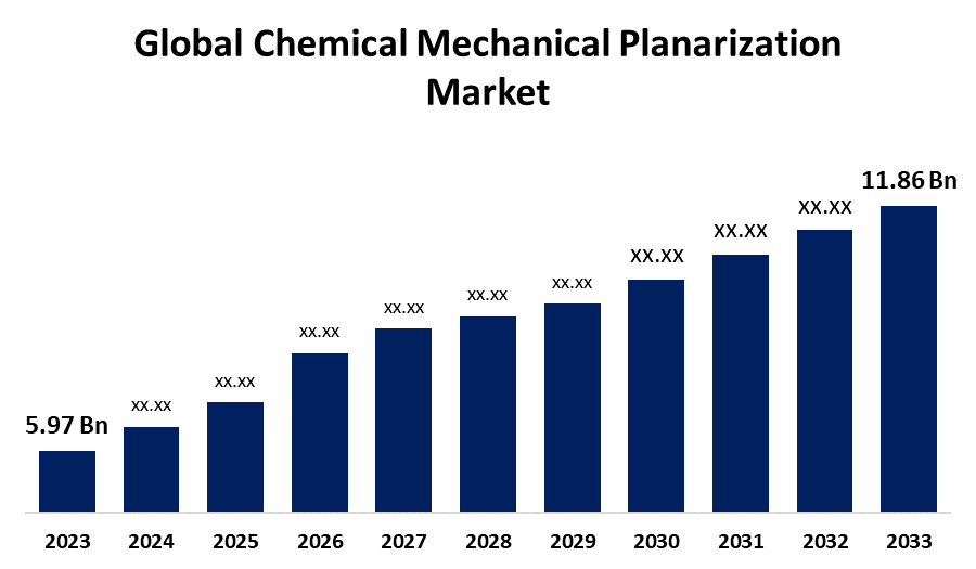
- The Global Chemical Mechanical Planarization Market Size Was Valued at USD 5.97 Billion in 2023
- The Market Size is Growing at a CAGR of 7.11% from 2023 to 2033
- The Worldwide Chemical Mechanical Planarization Market Size is Expected to Reach USD 11.86 Billion by 2033
- Asia-Pacific is Expected to Grow the fastest during the forecast period.
Get more details on this report -
The Chemical Mechanical Planarization Market Size is Anticipated to Exceed USD 11.86 Billion by 2033, Growing at a CAGR of 7.11% from 2023 to 2033.
CHEMICAL MECHANICAL PLANARIZATION MARKET REPORT OVERVIEW
The process of planarizing and smoothing surfaces, which typically consist of two or more distinct materials, is known as chemical mechanical planarization, or CMP. The process of adjusting the height disparities between neighboring structures is known as local planarization, whereas the process of adjusting the height differences across the whole substrate surface is known as global planarization. Global planarization can only be accomplished via CMP surface processing technology. In the semiconductor industry, planarizing thin films is often accomplished through the use of CMP. Metals, polysilicon, and dielectrics are among the materials that can be treated. Surfaces that are polished are of excellent quality. Powerful and highly integrated circuit components are developed with the help of CMP, which also makes multilayer systems manufacture possible. The CMP technique was first developed to planarize silica, the most widely used dielectric material, using the concepts of glass polishing in the fabrication of microelectronics. More complex CMP processes are being introduced as the demand for microelectronic device processing power rises. This is because advanced materials like polymeric dielectrics and metal interconnects like Cu and Ge are being used in applications where efficiency and frequency are crucial, like photovoltaics, automotive technology, and radio frequency (RF). CMP procedures are primarily employed at IMPT as a transitional stage in the building of multilayer electromagnetic actuators and sensors. Involves simultaneous chemical and mechanical procedures to eliminate surplus material, increase uniformity, and enable precise patterning of integrated circuits.
Report Coverage
This research report categorizes the market for the global chemical mechanical planarization market based on various segments and regions forecasts revenue growth and analyzes trends in each submarket. The report analyses the key growth drivers, opportunities, and challenges influencing the global chemical mechanical planarization market. Recent market developments and competitive strategies such as expansion, product launch, and development, partnership, merger, and acquisition have been included to draw the competitive landscape in the market. The report strategically identifies and profiles the key market players and analyses their core competencies in each sub-segment of the global chemical mechanical planarization market.
Global Chemical Mechanical Planarization Market Report Coverage
| Report Coverage | Details |
|---|---|
| Base Year: | 2023 |
| Market Size in 2023: | USD 5.97 Billion |
| Forecast Period: | 2023 – 2033 |
| Forecast Period CAGR 2023 – 2033 : | 7.11% |
| 023 – 2033 Value Projection: | USD 11.86 Billion |
| Historical Data for: | 2019 - 2022 |
| No. of Pages: | 220 |
| Tables, Charts & Figures: | 120 |
| Segments covered: | By Equipment, By Consumables, By Application |
| Companies covered:: | Lam Research Corporation, Intel Corporation, Samsung Electronics Co., Ltd., Micron Technology, Inc., Taiwan Semiconductor Manufacturing Company Limited, Okamoto Machine Tool Works, Ltd., Alpsitec SAS, Axus Technology, Revasum, GlobalFoundries Inc, Hitachi Chemical Co., Ltd., Ebara Corporation, Versum Materials, Inc., DuPont Electronic Solutions, BASF SE, and Others |
| Pitfalls & Challenges: | COVID-19 Empact, Challenge, Future, Growth, & Analysis |
Get more details on this report -
DRIVING FACTORS:
The chemical mechanical planarization market is driven by the growing usage of planarization in the semiconductor industry.
In the semiconductor sector, CMP is commonly utilized for metal layer planarization, and oxide dielectric planarization microelectromechanical systems are made with it. The semiconductor business is being driven by an increase in demand for mobile devices, PCs, and molded interconnect devices (MIDs). As a result, more chips supporting different functionalities in electronic devices are being produced. Therefore, growth in the semiconductor sector is probably going to drive the CMP market during the course of the forecast.
RESTRAINING FACTORS
The market expansion could be limited by reducing defects in different CMP methods.
The device performance, yield, and difficulties in high-volume manufacture were impacted by the strict need for precise process control and defect elimination in various CMP techniques. Furthermore, the intricacy of refined materials propels the advancement of CMP consumables. The manufacturing of CMP equipment and consumables is reduced globally as a result of increased quality control over new consumables, which also affects the production line and process window.
Market Segmentation
The chemical mechanical planarization market share is classified into equipment, consumables, and applications.
The polishing & grinding segment has the highest share of the market over the forecast period.
Based on equipment, the chemical mechanical planarization is classified into polishing & grinding, slurry testing, and laboratory. The polishing and grinding equipment sector is anticipated to dominate the global market. The goal of chemical mechanical paired grinding is to significantly reduce defects under practical and cost-effective operating circumstances. To attain extremely high degrees of planarity and eliminate material, chemical mechanical polishing is employed. It polishes semiconductor wafers or other substrates using mechanical abrasion and chemical oxidation. Technologies for grinding and polishing are used in many industries and provide products with more value. Different kinds of polishing and grinding procedures have been created and applied to industrial locations in addition to standard processing methods. Though they have been marketed for a long time, polishing and grinding procedures can still be developed technically and intellectually.
The surge in demand for the slurry segment can enhance the market growth during the forecast period.
Based on consumables, the chemical mechanical planarization is classified into slurry and pad conditioners. The slurry sector is expected to hold the greatest share of the global market. Slurries are liquid dispersions used in chemical mechanical planarization that include micro-abrasive grains and active chemicals. Usually, they are composed of a powdered abrasive that is nanosized and mixed with a solution that reacts chemically. The material is softened by chemical etching, but it is removed by mechanical abrasion, flattening the topographic characteristics and smoothing the surface. Throughout the compound semiconductor production process, CMP pads and slurries are combined and applied repeatedly to a polishing tool to planarize both die-level and wafer-level topography. The percentage of slurry that truly enters the area between the wafer and the pad to participate in the polish is known as the slurry usage efficiency. Based on various operating variables such as applied wafer pressure, relative pad wafer velocity, slurry flow rate, and pad surface texture, the results indicate that η varies between 2 and 22%.
The integrated circuits segment is the largest share of the market throughout the forecast period.
Based on application, the chemical mechanical planarization is classified into integrated circuits, optics, compound semiconductors, MEMS & NEMS. Integrated circuits have become an independent field within the semiconductor and microelectronics industries. They consist of incredibly dense arrays made up of hundreds to millions of discrete electrical elements that are placed on tiny semiconducting substrates. Silicon (Si) and, to a lesser extent, gallium arsenide (GaAs) have been the primary materials used in microelectronic substrates for decades, despite the fact that focused research and development have produced innumerable novel semiconductors appropriate for IC manufacture. The term "chip" is frequently used to refer to integrated circuits, which are actually substrate materials that have been removed from semiconductor ingots. Although these wafers are obtained by means of extraordinarily precise methods (such as diamond wire saw cutting). The goal of CMP is to planarize substrates for ultra-flatness following extraction, enhancing processes to meet the demands of a massive worldwide market.
Regional Segment Analysis of the Global Chemical Mechanical Planarization Market
- North America (U.S., Canada, Mexico)
- Europe (Germany, France, U.K., Italy, Spain, Rest of Europe)
- Asia-Pacific (China, Japan, India, Rest of APAC)
- South America (Brazil and the Rest of South America)
- The Middle East and Africa (UAE, South Africa, Rest of MEA)
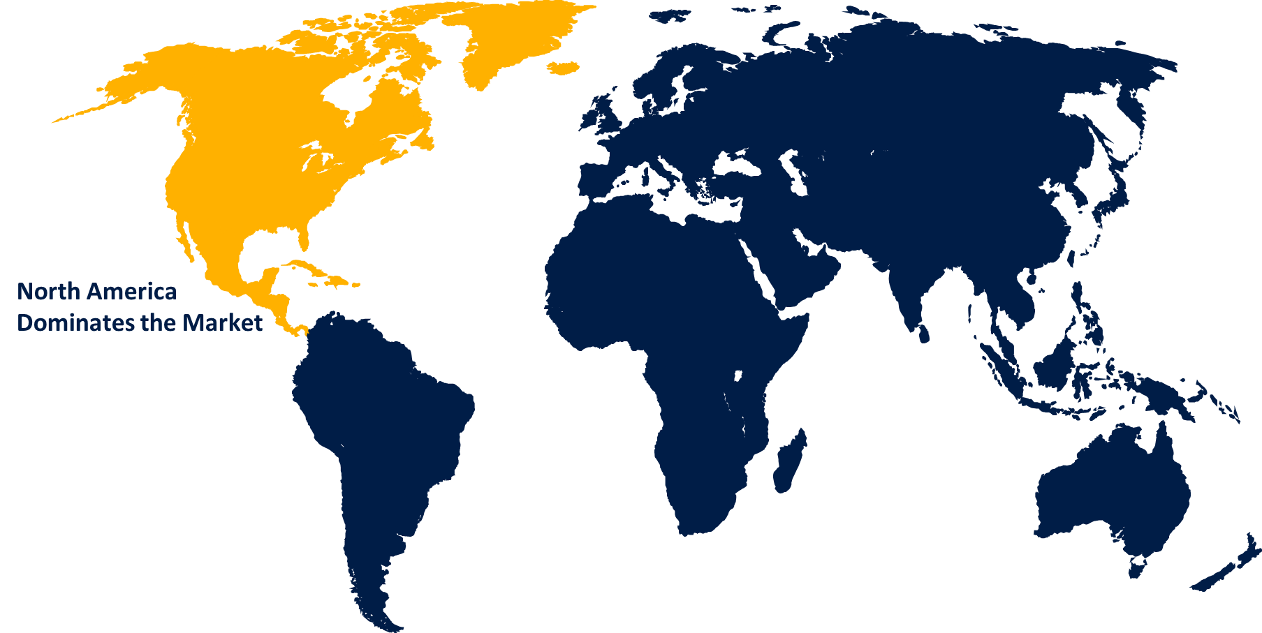
North America has the biggest share of the chemical mechanical planarization market throughout the forecast period.
Get more details on this report -
North America has a competitive advantage in the development of next-generation semiconductor technology because of its large R&D investments. The current environment is driving up demand for CMP technologies, which are essential to producing semiconductor wafers with high precision and consistency. Moreover, infrastructure support and supportive policies from the government solidify North America's standing as a major center for semiconductor manufacturing. Consequently, the region's tendencies in technology adoption and market expansion across numerous high-tech industries have made it an important player in the development of the worldwide CMP market.
The Asia-Pacific is the fastest-growing region over the projected timeframe.
The need for CMP technologies to ensure high yields and quality in semiconductor wafers is growing as Asia-Pacific's semiconductor production capacity rises. The area is more desirable for semiconductor manufacturing due to its favorable government laws, infrastructure investments, and skilled labor. As a result, Asia-Pacific is establishing itself as the CMP market region with the quickest rate of growth, which is boosting innovation and competition in the worldwide semiconductor sector.
Competitive Analysis:
The report offers the appropriate analysis of the key organizations/companies involved within the global chemical mechanical planarization market along with a comparative evaluation primarily based on their product offering, business overviews, geographic presence, enterprise strategies, segment market share, and SWOT analysis. The report also provides an elaborative analysis focusing on the current news and developments of the companies, which includes product development, innovations, joint ventures, partnerships, mergers & acquisitions, strategic alliances, and others. This allows for the evaluation of the overall competition within the market.
List of Key Companies
- Lam Research Corporation
- Intel Corporation
- Samsung Electronics Co., Ltd.
- Micron Technology, Inc.
- Taiwan Semiconductor Manufacturing Company Limited
- Okamoto Machine Tool Works, Ltd.
- Alpsitec SAS
- Axus Technology
- Revasum
- GlobalFoundries Inc
- Hitachi Chemical Co., Ltd.
- Ebara Corporation
- Versum Materials, Inc.
- DuPont Electronic Solutions
- BASF SE
- Others
Key Market Developments
- In July 2022, Entegris now deliver the industry's most extensive portfolio and improved operational capabilities for applications in the fab environment and throughout the semiconductor ecosystem with the inclusion of CMC Materials' array of products.
- In March 2022, with four manufacturing and research and development facilities around the country, FUJIFILM Electronic Materials, U.S.A., Inc. is a top provider of chemicals and advanced materials to the semiconductor industry. The company recently revealed that the $88 million expansion of its Mesa, California, electronic materials facility is now complete.
Key Target Audience
- Market Players
- Investors
- End-users
- Government Authorities
- Consulting And Research Firm
- Venture capitalists
- Value-Added Resellers (VARs)
Market Segment
This study forecasts revenue at global, regional, and country levels from 2020 to 2033. Spherical Insights has segmented the global chemical mechanical planarization market based on the below-mentioned segments:
Global Chemical Mechanical Planarization Market, By Equipment
- Polishing & Grinding
- Slurry Testing
- Laboratory
Global Chemical Mechanical Planarization Market, By Consumables
- Slurry
- Pad Conditioners
Global Chemical Mechanical Planarization Market, By Application
- Integrated Circuits
- Optics
- Compound Semiconductors
- MEMS & NEMS
Global Chemical Mechanical Planarization Market, By Regional
- North America
- US
- Canada
- Mexico
- Europe
- Germany
- Uk
- France
- Italy
- Spain
- Russia
- Rest of Europe
- Asia Pacific
- China
- Japan
- India
- South Korea
- Australia
- Rest of Asia Pacific
- South America
- Brazil
- Argentina
- Rest of South America
- Middle East & Africa
- UAE
- Saudi Arabia
- Qatar
- South Africa
- Rest of the Middle East & Africa
Frequently Asked Questions (FAQ)
-
1.What is the CAGR of the global chemical mechanical planarization market over the forecast period?The global chemical mechanical planarization market size is expected to grow from USD 5.97 Billion in 2023 to USD 11.86 Billion by 2033, at a CAGR of 7.09% during the forecast period 2023-2033.
-
2.Which region is expected to hold the highest share in the global chemical mechanical planarization market?North America is projected to hold the largest share of the global chemical mechanical planarization market over the forecast period.
-
3.Who are the top key players in the chemical mechanical planarization market?Lam Research Corporation, Intel Corporation, Samsung Electronics Co., Ltd, Micron Technology, Inc, Taiwan Semiconductor Manufacturing Company Limited, Okamoto Machine Tool Works, Ltd, Alpsitec SAS, Axus Technology, Revasum, GlobalFoundries Inc, Hitachi Chemical Co., Ltd, Ebara Corporation, Versum Materials, Inc, DuPont Electronic Solutions, BASF SE, and Others.
Need help to buy this report?