Global Gallium Arsenide (GaAs) Wafer Market Size, Share, and COVID-19 Impact Analysis, By Type (Polycrystalline, Single Crystal), By Application (Photovoltaic Devices, Wireless Communication, Mobile Devices, Optoelectronic Devices, Aerospace & Defense), and By Region (North America, Europe, Asia-Pacific, Latin America, Middle East, and Africa), Analysis and Forecast 2023 - 2033.
Industry: Automotive & TransportationGlobal Gallium Arsenide (GaAs) Wafer Market Insights Forecasts to 2033
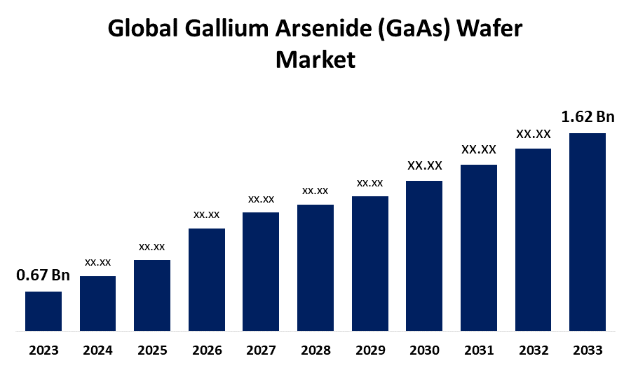
- The Global Gallium Arsenide (GaAs) Wafer Market Size was Valued at USD 0.67 Billion in 2023
- The Market Size is Growing at a CAGR of 9.23% from 2023 to 2033
- The Worldwide Gallium Arsenide (GaAs) Wafer Market Size is Expected to Reach USD 1.62 Billion by 2033
- North America is Expected to Grow the fastest during the forecast period.
Get more details on this report -
The Global Gallium Arsenide (GaAs) Wafer Market Size is Anticipated to Exceed USD 1.62 Billion by 2033, Growing at a CAGR of 9.23% from 2023 to 2033.
Market Overview
Gallium arsenide (GaAs) wafers are an important type of III-V direct bandgap semiconductor used in the production of semiconductors, barometers, light-emitting diodes (LEDs), thermometers, and electronic circuits. They are also used in the creation of solar cells. These wafers consist of gallium and arsenic that possess unique electrical and optical properties. Gallium arsenide (GaAs) wafers are manufactured by using techniques like molecular beam epitaxy (MBE), or metalorganic vapor phase epitaxy (MOVPE). These wafers have higher electron mobility than silicon, making them ideal for high-speed applications including barometers, high-speed transistors, and integrated circuits (ICs). As per the data provided by the Government of India Ministry of Power about 36.86 crore (LED) light bulbs are distributed across India under the Ujala Scheme and have garnered 407.92 Cr in market sales to date after the implementation of the Ujala scheme in 2015 which has saved up to 47,882 million kWh energy and reduced the CO2 emissions by 3.87 crore tons.
Report Coverage
This research report categorizes the market for the global gallium arsenide (GaAs) wafer market based on various segments and regions forecasts revenue growth and analyzes trends in each submarket. The report analyses the key growth drivers, opportunities, and challenges influencing the global gallium arsenide (GaAs) wafer market. Recent market developments and competitive strategies such as expansion, product launch, and development, partnership, merger, and acquisition have been included to draw the competitive landscape in the market. The report strategically identifies and profiles the key market players and analyses their core competencies in each sub-segment of the global gallium arsenide (GaAs) wafer market.
Global Gallium Arsenide (GaAs) Wafer Market Report Coverage
| Report Coverage | Details |
|---|---|
| Base Year: | 2023 |
| Market Size in 2023: | USD 0.67 Billion |
| Forecast Period: | 2023-2033 |
| Forecast Period CAGR 2023-2033 : | 9.23% |
| 2033 Value Projection: | USD 1.62 Billion |
| Historical Data for: | 2019-2022 |
| No. of Pages: | 267 |
| Tables, Charts & Figures: | 115 |
| Segments covered: | By Type, By Application, and By Region |
| Companies covered:: | Freiberger Compound Materials GmbH, Nanografi Nano Technology, Azelis Group, American Elements, DOWA Holdings Co., Ltd., AXT Inc., CrysTec GmbH, Atecom Technology Co., Ltd., Logitech Limited, IQE PLC, nanoPHAB B.V., CMC Microsystems, Intelligent Epitaxy Technology, Inc. (IntelliEPI), ALB Materials Inc., PlutoSemi Co., Ltd., and Others |
| Pitfalls & Challenges: | COVID-19 Empact, Challenge, Future, Growth, & Analysis |
Get more details on this report -
Driving Factors
Gallium Arsenide (GaAs) wafers have better electron conductivity than silicon, allowing faster processing of electronic signals. This makes GaAs perfect for high-frequency and high-speed applications, including microwave devices and radio frequency (RF) components. In addition, GaAs wafers have a straight bandgap, which makes them important for photovoltaic devices such as solar cells, LEDs, and laser diodes because they provide efficient light output. In addition, GaAs have strong radiation resistance, improving their reliability and performance in aerospace and defense applications where the materials are placed in harsh environments.
Restraining Factors
GaAs wafers face many challenges, such as high cost due to complex manufacturing processes, brittleness, and limited scalability compared to silicon wafers and this makes GaAs less competitive where cost is a major concern. GaAs are more toxic than silicon, raising environmental and safety concerns during production and disposal. These drawbacks, together with their toxicity, pose challenges to the widespread use of GaAs wafers in the semiconductor industry.
Market Segmentation
The global gallium arsenide (GaAs) wafer market share is classified into type and application.
- The single crystal segment is expected to hold the largest share of the global gallium arsenide (GaAs) wafer market during the forecast period.
Based on the type, the global gallium arsenide (GaAs) wafer market is divided into polycrystalline, and single crystal. Among these, the single crystal segment is expected to hold the largest share of the global gallium arsenide (GaAs) wafer market during the forecast period. The single-crystal GaAs wafer market is predicted to grow rapidly owing to its importance in high-performance electronic applications. Its uniform crystal structure provides good electron mobility, thermal stability, and low signal noise, which are important for high-frequency devices. The need for high-quality GaAs wafers is growing with the demand for faster and more reliable networks such as 5G. Single-crystal GaAs wafers are also valuable in photovoltaic applications such as lasers, LEDs, and solar cells. Improvements in manufacturing processes are driving demand for these wafers.
The wireless communication segment is expected to grow at the fastest CAGR in the global gallium arsenide (GaAs) wafer market during the forecast period.
Based on the application, the global gallium arsenide (GaAs) wafer market is divided into photovoltaic devices, wireless communication, mobile devices, optoelectronic devices, and aerospace & defense. Among these, the wireless communication segment is expected to grow at the fastest CAGR in the global gallium arsenide (GaAs) wafer market during the forecast period. Growth in the wireless communications segment is driven by increasing demand for high-performance radio frequency components, especially with the spread of 5G networks around the world. GaAs wafers are invaluable for their excellent electron conductivity and high-frequency continuity, which are essential for advanced RF devices such as amplifiers, switches, and antennas used in mobile phones and base stations. As the world becomes more connected, the adoption of GaAs-based materials will increase exponentially, enabling next-generation connectivity systems.
Regional Segment Analysis of the Global Gallium Arsenide (GaAs) Wafer Market
- North America (U.S., Canada, Mexico)
- Europe (Germany, France, U.K., Italy, Spain, Rest of Europe)
- Asia-Pacific (China, Japan, India, Rest of APAC)
- South America (Brazil and the Rest of South America)
- The Middle East and Africa (UAE, South Africa, Rest of MEA)
Asia Pacific is anticipated to hold the largest share of the global gallium arsenide (GaAs) wafer market over the predicted timeframe.

Get more details on this report -
Asia Pacific is anticipated to hold the largest share of the global gallium arsenide (GaAs) wafer market over the predicted timeframe. This dominance comes from the region’s strong manufacturing industry, which is a global leader in producing smartphones, consumer electronics, and communications devices. Rapid expansion of 5G networks, demand for high-frequency RF components in the region continues to boost demand for GaAs wafers. Furthermore, the presence of leading semiconductor manufacturers and ongoing investments in advanced technologies such as photovoltaics and optoelectronics contribute to the regional market share.
North America is expected to grow at the fastest pace in the global gallium arsenide (GaAs) wafer market during the forecast period. This growth is primarily driven by the strong demand for advanced technologies in the wireless communications, airspace, and defense sectors in the United States. Also, the region is a significant hub for innovation in high-frequency RF components, photoelectronic, and semiconductor technologies. Furthermore, continued investment in research and development, as well as increasing adoption of 5G networks and other next-generation communication technologies, is expected to drive significant growth in the North American GaAs wafer market.
Competitive Analysis:
The report offers the appropriate analysis of the key organizations/companies involved within the global gallium arsenide (GaAs) Wafer market along with a comparative evaluation primarily based on their product offering, business overviews, geographic presence, enterprise strategies, segment market share, and SWOT analysis. The report also provides an elaborative analysis focusing on the current news and developments of the companies, which includes product development, innovations, joint ventures, partnerships, mergers & acquisitions, strategic alliances, and others. This allows for the evaluation of the overall competition within the market.
List of Key Companies
- Freiberger Compound Materials GmbH
- Nanografi Nano Technology
- Azelis Group
- American Elements
- DOWA Holdings Co., Ltd.
- AXT Inc.
- CrysTec GmbH
- Atecom Technology Co., Ltd.
- Logitech Limited
- IQE PLC
- nanoPHAB B.V.
- CMC Microsystems
- Intelligent Epitaxy Technology, Inc. (IntelliEPI)
- ALB Materials Inc.
- PlutoSemi Co., Ltd.
- Others
Key Target Audience
- Market Players
- Investors
- End-users
- Government Authorities
- Consulting And Research Firm
- Venture capitalists
- Value-Added Resellers (VARs)
Recent Developments
- In May 2022, The MOSIS Service of the Information Sciences Institute, University of Southern California, has signed an agreement with WIN Semiconductors Corp. to speed the development of GaAs wafer and GaN monolithic microwave integrated circuits.
- In December 2022, Marktech Optoelectronics launches new 2.6µm Extended InGaAs Photodiode Photodetectors which are Vis-NIR-SWIR and NIR-SWIR-Extended SWIR.
Market Segment
This study forecasts revenue at global, regional, and country levels from 2020 to 2033. Spherical Insights has segmented the global gallium arsenide (GaAs) wafer market based on the below-mentioned segments:
Global Gallium Arsenide (GaAs) Wafer Market, By Type
- Polycrystalline
- Single Crystal
Global Gallium Arsenide (GaAs) Wafer Market, By Application
- Photovoltaic Devices
- Wireless Communication
- Mobile Devices
- Optoelectronic Devices
- Aerospace & Defense
Global Gallium Arsenide (GaAs) Wafer Market, Regional
- North America
- US
- Canada
- Mexico
- Europe
- Germany
- UK
- France
- Italy
- Spain
- Russia
- Rest of Europe
- Asia Pacific
- China
- Japan
- India
- South Korea
- Australia
- Rest of Asia Pacific
- South America
- Brazil
- Argentina
- Rest of South America
- Middle East & Africa
- UAE
- Saudi Arabia
- Qatar
- South Africa
- Rest of the Middle East & Africa
Frequently Asked Questions (FAQ)
-
1. Which are the key companies that are currently operating within the market?Freiberger Compound Materials GmbH, Nanografi Nano Technology, Azelis Group, American Elements, DOWA Holdings Co., Ltd., AXT Inc., CrysTec GmbH, Atecom Technology Co., Ltd., Logitech Limited, IQE PLC, nanoPHAB B.V., CMC Microsystems, Intelligent Epitaxy Technology, Inc. (IntelliEPI), ALB Materials Inc., PlutoSemi Co., Ltd., and Others.
-
2. What is the size of the global gallium arsenide (GaAs) wafer market?The Global Gallium Arsenide (GaAs) Wafer Market is expected to grow from USD 0.67 Billion in 2023 to USD 1.62 Billion by 2033, at a CAGR of 9.23% during the forecast period 2023-2033.
-
3. Which region is holding the largest share of the market?Asia Pacific is anticipated to hold the largest share of the global gallium arsenide (GaAs) wafer market over the predicted timeframe.
Need help to buy this report?