Global Indium Phosphide Wafer Market Size, Share, and COVID-19 Impact Analysis, By Diameter (2 Inches, 3 Inches, and 4 Inches and above), By Type (P-Type and N-Type), By Application (Consumer Electronics, Telecommunication, Healthcare), and By Region (North America, Europe, Asia-Pacific, Latin America, Middle East, and Africa), Analysis and Forecast 2023 - 2033.
Industry: Chemicals & MaterialsGlobal Indium Phosphide Wafer Market Insights Forecasts to 2033
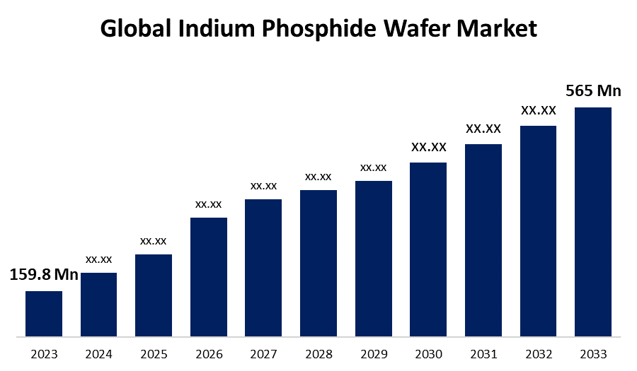
- The Global Indium Phosphide Wafer Market Size was Valued at USD 159.8 Million in 2023
- The Market Size is Growing at a CAGR of 13.46% from 2023 to 2033
- The Worldwide Indium Phosphide Wafer Market Size is Expected to Reach USD 565 Million by 2033
- Europe is Expected to Grow the fastest during the forecast period.
Get more details on this report -
The Global Indium Phosphide Wafer Market Size is Anticipated to Exceed USD 565 Million by 2033, Growing at a CAGR of 13.46% from 2023 to 2033.
Market Overview
An indium phosphide wafer (InP) is a binary semiconductor made of indium (In) and phosphorus (P). It belongs to a group of materials known as III-V Semiconductors. It is used in high-power and high-frequency electronics and photonics applications. Indium phosphide has a superior electron velocity than more common semiconductors such as silicon and gallium arsenide.
Indium phosphide (InP) wafers are produced by techniques like metal-organic chemical vapor deposition (MOCVD) or molecular beam epitaxy (MBE). These wafers are then processed and fabricated into various electronic components, such as high-electron-mobility transistors (HEMTs), laser diodes, photodetectors, and integrated circuits (ICs).
Due to the high electron mobility, InP-based devices offer faster operation speeds, making them ideal for high-frequency and high-speed electronic devices. Additionally, the direct bandgap of InP allows efficient photon emission and absorption, positioning these wafers as the preferred choice for optoelectronic applications such as photonic integrated circuits, lasers, and high-efficiency solar cells. The thermal stability of InP contributes to its reliability in demanding environments.
There has been several developments in the indium phosphide wafer (InP) market recently. For instance, In September 2024, Move2THz, a European research and industry consortium led by Soitec, commenced work to develop a future generation of high-frequency semiconductors based on indium phosphide (InP).
Report Coverage
This research report categorizes the market for the global indium phosphide wafer market based on various segments and regions forecasts revenue growth and analyzes trends in each submarket. The report analyses the key growth drivers, opportunities, and challenges influencing the global indium phosphide wafer market. Recent market developments and competitive strategies such as expansion, product launch, and development, partnership, merger, and acquisition have been included to draw the competitive landscape in the market. The report strategically identifies and profiles the key market players and analyses their core competencies in each sub-segment of the global indium phosphide wafer market.
Global Indium Phosphide Wafer Market Report Coverage
| Report Coverage | Details |
|---|---|
| Base Year: | 2023 |
| Market Size in 2023: | USD 159.8 Million |
| Forecast Period: | 2023 - 2033 |
| Forecast Period CAGR 2023 - 2033 : | 13.46% |
| 2033 Value Projection: | USD 565 Million |
| Historical Data for: | 2019-2022 |
| No. of Pages: | 231 |
| Tables, Charts & Figures: | 110 |
| Segments covered: | By Diameter, By Type, By Application, By Region |
| Companies covered:: | AXT Inc., Wafer World Inc., Logitech Ltd., IntelliEPI Inc., MTI Corporation, JX Nippon Mining & Metals Corporation, Beijing JiYa Semiconductor Material Co. Ltd., Sumitomo Electric Industries Ltd., Wafer Technology Ltd., Western Minmetals (sc) Corporation, CMK Ltd., Century Goldray Semiconductor Co. Ltd., PAM-XIAMEN, Umicore, Furuya Metal Co. Ltd., and Others |
| Pitfalls & Challenges: | Covid 19 Impact Challanges, Future, Growth and Analysis |
Get more details on this report -
Driving Factors
The market growth for indium phosphide (InP) wafers is driven by their superior electronic and photonic properties, which include high electron mobility and a direct bandgap. These characteristics make InP wafers crucial for high-speed and high-frequency electronic devices. The increasing demand for advanced communication systems, including 3G, 5G, LTE infrastructure, and photonic integrated circuits, further boosts the market. Additionally, the expanding applications in optoelectronics, such as high-efficiency solar cells and laser technologies, contribute to the market's upward trajectory. The continuous advancements in semiconductor technology and research and development in consumer electronics also play a pivotal role in fuelling the growth of the global indium phosphide wafers market.
Restraining Factors
The complexity of the manufacturing process and the scarcity of raw materials increase the cost of production of InP wafers. Additionally, the market might face competition from alternative semiconductors like silicon and gallium arsenide (GaAs), which offer cost-effective solutions for some applications. The limited availability of advanced fabrication facilities capable of handling InP wafers also restricts widespread adoption. These challenges could hinder the market from achieving its full growth potential.
Market Segmentation
The global indium phosphide wafer market share is classified into diameter, type, and application.
- The 4-inch and above segment is expected to hold the largest share of the global indium phosphide wafer market during the forecast period.
Based on the diameter, the global indium phosphide wafer market is divided into 2 inches, 3 inches, and 4 inches and above. Among these, the 4-inch and above segment is expected to hold the largest share of the global indium phosphide wafer market during the forecast period. Larger diameter wafers allow for higher production efficiency, as more chips can be fabricated from a single wafer, reducing the cost per unit. Additionally, the advancements in semiconductor manufacturing equipment have made processing larger wafers more feasible and cost-effective. The increased adoption of 4-inch and above wafers in high-frequency and high-power applications, such as telecommunications and photonic integrated circuits, also contributes to this segment's leading position in the market.
- The n-type segment is expected to hold the largest share of the global indium phosphide wafer market during the forecast period.
Based on the type, the global indium phosphide wafer market is divided into p-type and n-type. Among these, the n-type segment is expected to hold the largest share of the global indium phosphide wafer market during the forecast period. The n-type indium phosphide wafer has superior electron mobility and saturation velocity of n-type wafers, which make them ideal for high-speed and high-frequency applications. N-type wafers are extensively utilized in advanced electronic and optoelectronic devices, such as high-speed transistors, lasers, and photodetectors. Additionally, their high thermal stability and excellent performance under varying environmental conditions further enhance their attractiveness for industrial and commercial applications. The broad adoption in critical sectors like telecommunications and defense contributes to the n-type segment.
- The consumer electronics segment is expected to grow at the fastest CAGR in the global indium phosphide wafer market during the forecast period.
Based on application, the global indium phosphide wafer market is divided into consumer electronics, telecommunication, and healthcare. Among these, the consumer electronics segment is expected to grow at the fastest CAGR in the global indium phosphide wafer market during the forecast period. This rapid growth is driven by the increasing demand for high-performance, compact, and energy-efficient devices. Indium phosphide wafers are integral for advanced electronic components such as high-speed transistors, lasers, and photodetectors used in smartphones, tablets, and wireless communication devices. The ongoing advancements in technology and consumer preferences for enhanced functionality and connectivity are accelerating the adoption of InP wafers. Additionally, the expanding market for wearable devices and the Internet of Things (IoT) continues to boost the growth prospects in the consumer electronics sector.
Regional Segment Analysis of the Global Indium Phosphide Wafer Market
- North America (U.S., Canada, Mexico)
- Europe (Germany, France, U.K., Italy, Spain, Rest of Europe)
- Asia-Pacific (China, Japan, India, Rest of APAC)
- South America (Brazil and the Rest of South America)
- The Middle East and Africa (UAE, South Africa, Rest of MEA)
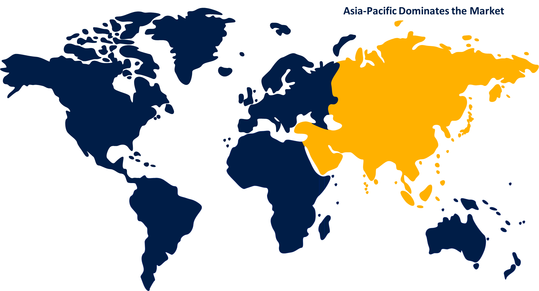
Asia-Pacific is anticipated to hold the largest share of the global indium phosphide wafer market over the predicted timeframe.
Get more details on this report -
Asia-Pacific is anticipated to hold the largest share of the global indium phosphide wafer market over the predicted timeframe. This region has the status of the global hub for semiconductor manufacturing, with the presence of leading electronics companies. The high number of industries and significant investments in technology and infrastructure across countries such as China, Japan, South Korea, Taiwan, and India drive the demand for advanced semiconductor materials. Additionally, the growing consumer electronics market, driven by a tech-savvy population, boosts the need for high-performance components like InP wafers. The favorable government policies, funding for research and development, and tax benefits for start-ups in the semiconductor sector further support the market's growth.
Europe is expected to grow at the fastest pace in the global indium phosphide wafer market during the predicted timeframe. Europe has a strong focus on innovation and advancements in semiconductor technology. The European Union's substantial investments in research and development, combined with supportive governmental policies, foster a thriving environment for the semiconductor industry. Additionally, the increasing demand for high-speed communication networks and advanced electronics in various sectors, including automotive, aerospace, and healthcare, further propels the market. The rising adoption of photonic integrated circuits and other optoelectronic applications also contributes to the rapid market expansion.
Competitive Analysis:
The report offers the appropriate analysis of the key organizations/companies involved within the global indium phosphide wafer market along with a comparative evaluation primarily based on their product offering, business overviews, geographic presence, enterprise strategies, segment market share, and SWOT analysis. The report also provides an elaborative analysis focusing on the current news and developments of the companies, which includes product development, innovations, joint ventures, partnerships, mergers & acquisitions, strategic alliances, and others. This allows for the evaluation of the overall competition within the market.
List of Key Companies
- AXT Inc.
- Wafer World Inc.
- Logitech Ltd.
- IntelliEPI Inc.
- MTI Corporation
- JX Nippon Mining & Metals Corporation
- Beijing JiYa Semiconductor Material Co. Ltd.
- Sumitomo Electric Industries Ltd.
- Wafer Technology Ltd.
- Western Minmetals (sc) Corporation
- CMK Ltd.
- Century Goldray Semiconductor Co. Ltd.
- PAM-XIAMEN
- Umicore
- Furuya Metal Co. Ltd.
- Others
Key Target Audience
- Market Players
- Investors
- End-users
- Government Authorities
- Consulting And Research Firm
- Venture capitalists
- Value-Added Resellers (VARs)
Recent Developments
- In January 2024, SMART Photonics, a foundry for photonic integrated circuits, scaled up its production of photonic chips by transferring its entire production capability from 3-inch to 4-inch wafer substrates. According to the company, SMART Photonics is among the first photonic integrated circuit foundries offering 4-inch indium phosphide wafer production.
- In July 2024, Netherlands-based photonic chip accelerator PhotonDelta opened an office in California with the goal of growing the photonic chip industry by facilitating collaboration between European and North American organizations.
Market Segment
This study forecasts revenue at global, regional, and country levels from 2020 to 2033. Spherical Insights has segmented the global indium phosphide wafer market based on the below-mentioned segments:
Global Indium Phosphide Wafers Market, By Diameter
- 2 Inches
- 3 Inches
- 4 Inches and above
Global Indium Phosphide Wafers Market, By Type
- P-Type
- N-Type
Global Indium Phosphide Wafers Market, By Application
- Consumer Electronics
- Telecommunication
- Healthcare
Global Indium Phosphide Wafer Market, Regional
- North America
- US
- Canada
- Mexico
- Europe
- Germany
- UK
- France
- Italy
- Spain
- Russia
- Rest of Europe
- Asia Pacific
- China
- Japan
- India
- South Korea
- Australia
- Rest of Asia Pacific
- South America
- Brazil
- Argentina
- Rest of South America
- Middle East & Africa
- UAE
- Saudi Arabia
- Qatar
- South Africa
- Rest of the Middle East & Africa
Frequently Asked Questions (FAQ)
-
1. Which are the key companies that are currently operating within the market?AXT Inc., Wafer World Inc., Logitech Ltd., IntelliEPI Inc., MTI Corporation, JX Nippon Mining & Metals Corporation, Beijing JiYa Semiconductor Material Co. Ltd., Sumitomo Electric Industries Ltd., Wafer Technology Ltd., Western Minmetals (sc) Corporation, CMK Ltd., Century Goldray Semiconductor Co. Ltd., PAM-XIAMEN, Umicore, Furuya Metal Co. Ltd., and Others.
-
2. What is the size of the global indium phosphide wafer market?The Global Indium Phosphide Wafer Market is expected to grow from USD 159.8 Million in 2023 to USD 565 Million by 2033, at a CAGR of 13.46% during the forecast period 2023-2033.
-
3. Which region is holding the largest share of the market?Asia-Pacific is anticipated to hold the largest share of the global indium phosphide wafer market over the predicted timeframe.
Need help to buy this report?